IBM Unveils Revolutionary Sub-1 Nanometer Chip Architecture Technology
IBM Announces Groundbreaking Sub-1 Nanometer Chip Technology
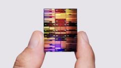
International Business Machines Corporation has unveiled what the company claims represents the world's first commercially viable approach to sub-1 nanometer chip technology. This significant advancement in semiconductor engineering demonstrates IBM's commitment to pushing the boundaries of microprocessor miniaturization beyond previously achieved limits.
Understanding the Innovation Behind Sub-1 Nanometer Chip Technology
The newly developed sub-1 nanometer chip technology employs an innovative architectural approach that fundamentally reimagines how semiconductor layers are constructed. Rather than traditional flat designs, IBM has implemented a vertical stacking methodology that optimizes space utilization and enhances computational efficiency. This breakthrough represents a substantial leap forward in the evolution of semiconductor manufacturing processes.
The Vertical Stacking Architecture Explained
The architectural design resembles a residential apartment complex, with multiple processing layers stacked vertically atop one another. This three-dimensional configuration enables manufacturers to increase transistor density without proportionally expanding the chip's physical footprint. The innovative arrangement allows for more sophisticated data processing capabilities within increasingly constrained physical dimensions, addressing one of the semiconductor industry's most persistent engineering challenges.
Technical Specifications and Performance Advantages
IBM's sub-1 nanometer chip technology incorporates advanced materials and manufacturing techniques that were previously considered impractical for mass production. The stacked configuration provides multiple functional advantages, including improved heat dissipation, reduced power consumption, and enhanced signal integrity between processing layers. These technical improvements collectively contribute to superior overall chip performance compared to conventional flat architecture designs.
The innovative approach addresses critical limitations encountered in previous generations of semiconductor technology. By implementing vertical integration at the nanometer scale, IBM has successfully overcome fundamental physics constraints that previously restricted further miniaturization. This represents a watershed moment in semiconductor engineering, comparable to earlier industry breakthroughs that initially seemed impossible to achieve.
Production Timeline and Market Availability
Despite the significant technological achievement, IBM has emphasized that practical implementation of sub-1 nanometer chip technology in commercial products remains years away. The company projects that manufacturing processes must undergo extensive refinement and optimization before full-scale production becomes feasible. Current manufacturing facilities and equipment require substantial upgrades to support the precision demands necessary for consistent production at this scale.
Development Milestones and Future Roadmap
IBM's development roadmap indicates that prototype testing and validation will occupy the near-term future, with incremental production scaling planned for subsequent phases. The company has not disclosed specific timelines for commercial deployment, recognizing that semiconductor manufacturing at the sub-nanometer scale presents unprecedented complexity. Researchers anticipate that technological and infrastructural preparations will require several years of dedicated effort.
Industry Implications and Competitive Landscape
This breakthrough positions IBM as a technological leader in next-generation semiconductor development. Other major semiconductor manufacturers, including Intel and Taiwan Semiconductor Manufacturing Company, have pursued comparable miniaturization objectives through alternative architectural approaches. IBM's sub-1 nanometer chip technology announcement reignites competition within the industry to achieve and commercialize revolutionary chip designs capable of unprecedented processing performance.
The competitive pressure to achieve sub-nanometer manufacturing capabilities reflects the technology sector's continued demand for enhanced computational power and improved energy efficiency. Data centers, artificial intelligence applications, and consumer electronics all require increasingly powerful processors. IBM's innovation directly addresses this market need by demonstrating a viable pathway toward next-generation semiconductor technology.
Manufacturing Challenges and Technical Hurdles
Producing reliable chips utilizing sub-1 nanometer chip technology requires overcoming numerous manufacturing obstacles. Precision requirements at this scale demand equipment capable of atomic-level accuracy. Contamination control, thermal management, and material consistency present ongoing challenges that must be resolved before commercial viability becomes achievable. IBM's manufacturing experts must develop entirely new processes and quality assurance protocols to ensure consistent production outcomes.
Investment Requirements and Research Commitment
Transitioning from prototype development to production-ready manufacturing demands substantial capital investment and extended research commitment. IBM's semiconductor division has allocated significant resources toward advancing this technology through commercial deployment stages. The company's willingness to commit substantial financial resources demonstrates confidence in the commercial potential of sub-1 nanometer chip technology and its eventual market value.
Conclusion
IBM's announcement of breakthrough sub-1 nanometer chip technology represents a landmark achievement in semiconductor engineering. While commercial deployment remains years in the future, this innovation establishes a clear technological pathway for next-generation chip development. As manufacturing processes mature and production capabilities expand, this revolutionary technology will eventually transform computing capabilities across numerous applications and industries.